Original Link: https://www.anandtech.com/show/519
It seems like it has been an eternity since Intel made their first major dive into the low-cost CPU market. In 1998, at the Intel Developer Forum, Intel CEO Andy Grove outlined what would be a major step for the company, the idea of applying a single processor core design to multiple product segments in the market. In doing this, Intel effectively created what they liked to call the “Basic PCs,” which, at the time, referred to PCs that ranged from $800 - $1200 in price and provided “a base level of functionality with limited expandability to meet the core needs and affordability requirements common to many new home and business users.”
It was on that same day, March 4, 1998, that Intel released a new brand name for their upcoming CPU that was designed for this “Basic PC” market segment, the Celeron. A little over a month later, Intel made the official introduction of the Celeron CPU at 266MHz for a price under $200.
The 66MHz FSB Celeron made its introduction on the same day that the Pentium II gained 100MHz FSB support provided by the 440BX chipset for the 350 and 400MHz parts. At the time, little attention was paid to the performance benefits provided by the 100MHz FSB frequency over the Celeron’s and older Pentium II’s 66MHz FSB speed.
By combining the fact that the Celeron used the “slower” 66MHz FSB as well as the fact that the first Celerons had no L2 cache, Intel attempted to truly differentiate the Celeron from its Pentium II brother. Intel did not want anyone using the Celeron as the basis for a high performance system as that was what the Pentium II was for and the profit margins on the Pentium II were greater than they were on the Celeron.
This original Celeron was a success among hardware enthusiasts because the 266MHz Celeron could easily make it up to 400MHz by simply increasing the FSB frequency from 66MHz to 100MHz. At 400MHz, the Celeron offered gaming performance virtually equivalent to that of the Pentium II 400, and thus, the Celeron became the ideal gaming solution.
With no L2 cache, the Celeron suffered incredibly in business/office application benchmarks and while the majority of gamers were enjoying Intel’s extremely overclockable Celeron solution, the Celeron came out looking very under par since most magazines use a combination of business and office applications to measure performance. By removing the L2 cache from the Celeron’s SEPP card, Intel could cut costs while establishing a clear performance difference between their low-end (Celeron) and their high-end (Pentium II) chips.
In spite of the fact that business application performance isn’t that big of a deal, Intel was forced to phase out the cacheless Celerons after hitting 300MHz. It was in August of 1998 that Intel introduced the Celeron A at 300 and 333MHz. The Celeron A improved on the weaknesses of the original Celeron by integrating 128KB of L2 cache running at core speed onto the die of the processor itself. This helped the business performance of the Celeron tremendously without affecting the price point of the processor since the Celeron’s 0.25-micron process allowed for the 128KB of L2 cache to be integrated onto the Celeron’s die without significantly increasing the cost of the CPU.
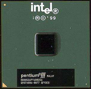
The Celeron A was introduced 19 months ago, and it has been with us ever since -- until today.
Introducing the Coppermine128
 The
first Celerons, without any L2 cache, were based on the Deschutes core that was
also used on the Pentium IIs.
The
first Celerons, without any L2 cache, were based on the Deschutes core that was
also used on the Pentium IIs.
The Deschutes core featured MMX instructions but didn’t have any SSE optimizations since the core was produced about 1.5 years before Intel ever unveiled their SSE instructions. The core itself was manufactured on Intel’s 0.25-micron process, which accounted for some of its initial overclocking success on the first Celerons, especially since it had no L2 cache to limit its clock speed potential.
The second generation Celerons, starting with the Celeron 300A and extending all the way up to the 533MHz part that was released in January of this year, made use of the Mendocino core which never appeared on another chip outside of the Celeron. Like the Deschutes core, the Mendocino core was built on Intel’s 0.25-micron process but added a full 128KB of on-die L2 cache which is where the Deschutes fell short. Other than that, the two cores are virtually identical.
For the first time since August 1998, the Celeron is receiving a new core, internally referred to as Coppermine128. This new core provides a huge change in comparison to the past two Celeron cores. Just like the original Celeron was a derivative of the Pentium II (it used the same core), the new Celeron is a derivative of the present day Pentium III processor.
If you recall, the Pentium III’s core is called the Coppermine, and what primarily defines the Coppermine is its 256KB Advanced Transfer Cache and the SSE instructions that have been with the Pentium III since day one.
The Coppermine128 core features the same advantages of the Pentium III’s core such as its SSE instructions and an Advanced Transfer Cache, but it drops the L2 cache size down to 128KB (hence the name Coppermine128) versus the 256KB found in the Pentium III’s Coppermine core.
While it may seem like the main improvement to the new Celerons is the addition of SSE instructions because, after all, the Celeron A also had 128KB of on-die L2 cache, there is more than meets the eye with this new Celeron.
Celeron 566/600 Specifications
· 0.18-micron Coppermine128 core
· 566/600MHz clock speed – 8.5/9.0x clock multiplier
· 32KB on-die L1 cache running at core speed
· 256-bit Advanced Transfer Cache - 128KB on-die L2 cache running at core speed
· Advanced System Buffering
· 370-pin FC-PGA Socket-370 GTL+ CPU interface running at 66MHz
· 1.50v core voltage
While we're about to start talking about most of the specifications, it is interesting to note that new 566/600MHz parts run at a core voltage of only 1.50v. Considering that their 600MHz FC-PGA Pentium III counterparts run at 1.60v, the 0.1v difference in core voltage can be attributed mostly to the 128KB of on-die L2 cache vs 256KB on the Pentium III.
By having a lower core voltage Intel can hopefully extend the line to some very high frequencies simply by increasing the core voltage as time goes on, the same potential is left to the users as far as overclocking is concerned.
Since the new Celerons are FC-PGA chips they will only work on Socket-370 motherboards that support FC-PGA processors and/or Socket-370 to Slot-1 converters that support FC-PGA CPUs.
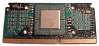
PPGA is old news
 As
we discussed at the beginning of this article, Intel’s Celeron 300A was the
first Celeron to feature an on-die L2 cache. Not only did the on-die L2 cache
run at clock speed and offer very low latency L2 access when compared to the
Pentium II’s off-die L2 cache (it’s obviously easier for the CPU to access something
that is contained within its die than something that is outside of its die),
but by moving the L2 cache onto the processor’s die, Intel also managed to eliminate
the need for the Celeron’s SEPP (Single Edge Processor Package) card.
As
we discussed at the beginning of this article, Intel’s Celeron 300A was the
first Celeron to feature an on-die L2 cache. Not only did the on-die L2 cache
run at clock speed and offer very low latency L2 access when compared to the
Pentium II’s off-die L2 cache (it’s obviously easier for the CPU to access something
that is contained within its die than something that is outside of its die),
but by moving the L2 cache onto the processor’s die, Intel also managed to eliminate
the need for the Celeron’s SEPP (Single Edge Processor Package) card.
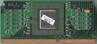
Intel eventually phased out the SEPP Celeron in favor of the PPGA (Plastic Pin Grid Array) Socket-370 version that, as the name implies and as we all are familiar with today, interfaces with a socket rather than a slot which helps to cut costs since Intel isn’t paying for the production of a PCB to mount the CPU on in addition to the CPU.
Around the time of the release of the Celeron 366, the first PPGA Socket-370 Celerons were made available, and by the time the 433MHz parts were released, finding an SEPP processor was virtually impossible.
The only problem with the PPGA packaging was that the heat generated by the CPU’s core never actually made contact with the heatsink on the outside of the package. Instead, the heat was dissipated through the package and then out to the heatsink. While this was fine for the older 266 – 533MHz parts, as the Celeron began to approach the 600MHz mark, removing the heat from the processor’s core in an efficient manner became increasingly difficult.
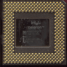
In order to get around this problem and pave the way for higher clock speed parts in the future, Intel began using a technology known as Flip Chip Pin Grid Array (FC-PGA) to package their processors starting with the Pentium III. This method of packaging, as the name implies, actually flips the die so that it is essentially resting against the base of the heatsink (under a protective layer, of course), but by doing this, it is easier to dissipate the amount of heat generated by these chips.
FC-PGA Pentium III
FC-PGA Celeron
The FC-PGA core, as well as the fact that the Coppermine128 is manufactured on Intel’s 0.18-micron Coppermine process, makes the 18W dissipated by the new Celeron running at 600MHz a very appetizing figure. To put it into perspective, at 18W, the Celeron 600 dissipates less heat than the newer Pentium III 550E (18.2W) and just barely more than the old Celeron 300A (17.8W).
128KB L2 does not equal 128KB L2
That’s a pretty bold statement don’t ya think? ;)
The fact of the matter is that the 128KB L2 cache on the new Celerons is not like the 128KB of L2 cache that has been on the Celeron die since the 300A.
If you remember back to our review of the Pentium III “Coppermine,” you will recall that one of the major improvements Intel made to the core was that the pathway to the on-die L2 cache was widened to 256-bits, which allowed for 11.7GB/s throughput when clocked at 733MHz.
The width of the path to the off-die L2 cache of the Pentium II and the original Pentium III (Katmai) was 1/4 the size at 64-bits, and even the width of the L2 cache data bus on the Celerons was only 64-bits.
Since the new Celerons are essentially 128KB variants of the newer Pentium IIIs, they also feature the same 256-bit L2 cache bus for 9.6GB/s of bandwidth at 600MHz on the Celeron to/from the L2 cache.
Processor Serial NumberUpdate: We have just recently been informed by Intel that the Processor Serial Number has been disabled on the new Celerons. Unlike turning the feature off in the BIOS, Intel physically disabled the feature in the hardware stating that it is more of a business level function and not intended for the entry-level market.
As we just mentioned, the new Celerons are essentially the same thing as the new Pentium IIIs with the exception that they are 66MHz FSB parts and feature 1/2 the L2 cache of the Pentium IIIs at 128KB.
The new Celerons will also feature Intel’s Processor Serial Number, which is essentially a unique identifier hard-coded into your CPU that can be accessed via a software interface for a number of purposes.
There was initially quite a bit of media hype surrounding the potential misuse of the Processor Serial Number, but most of that has since died down; there haven’t been any major, publicized uses for the feature.
Most motherboard manufacturers now provide a method to turn off the Processor Serial Number from within the BIOS for those that aren’t comfortable with the feature being enabled.
SSE
The Celeron 566/600 will be the first Celerons to feature Intel’s SSE instructions. For a brief recap of what SSE is, let’s take a look at our explanation of the technology from our original Pentium III review:
Intel had a lot of proving to do with the Pentium III's 70 Streaming SIMD Extensions (SSE), and among the tests they had to pass, proving that SSE wasn't just another MMX was one of them. At a first glance, it's easy to say that SSE would be another flop just like MMX, however if you look a little deeper into the two technologies you'll begin to notice quite a few differences.
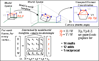
The name Streaming SIMD Extensions is indication in its own of the power of SSE, as we all remember from the introduction of the K6-2, SIMD is an extremely popular and powerful feature of the 3DNow! instructions. SIMD, or Single Instruction Multiple Data (in this case SIMD-FP as it applies to FPU instructions, whereas MMX offered SIMD-Int for Integer instructions) allows a single command (or instruction) to be applied to multiple sets of data simultaneously. The key to understanding the benefits of SIMD-FP instructions is the emphasis on the simultaneous execution of commonly used instructions such as multiplies, divides, and adds. The perfect example would be in the transfer of a simple cube in mathematical space to a 3D world as is illustrated by the diagram provided by Intel below:
Copyright 1999-2000 Intel CorporationThe 14 mults, 12 adds and 1 reciprocal function of the above transfer from model space to world space (mathematical space to 3D world space) could benefit greatly from the Pentium III's SSE as you're essentially executing the same instruction and applying it to multiple forms of data over and over again. The nature of SIMD-FP instructions allows for these instructions to be applied to multiple data structures processed by the CPU in a more timely manner, offering an actual improvement in performance.
While MMX did essentially the same thing for Integer values (whole numbers, i.e. 1, 2, 3…), most complex software such as 3D games, 3D rendering programs, image editing software, and even speech recognition software make use of Floating Point values (numbers with decimals, i.e. 0.0001), therefore there was a very tiny real-world performance improvement that Intel's MMX instructions brought to the table. At the same time, since floating point calculations already take an incredible amount of time to process, even on today's fastest x86 processors (relatively speaking, from the point of view of the CPU not the user); therefore, the application of SIMD to floating point operations as provided for by the Pentium III's SSE offers a greater tangible performance improvement than the application of SIMD to integer operations which are already quite fast on x86 systems.
Is the 66MHz FSB a Limitation?
Intel has always had the “habit” of planning ahead. While their decisions may sometimes seem to be made without any thought whatsoever, it is often the case that they make those decisions for a reason, but those benefits may not be seen until later down the road.
Following that theory, at the time the Celeron was released, there wasn’t a huge performance difference between a 66MHz FSB and a 100MHz FSB. This made many users think that it was unwise of Intel to move to the 100MHz FSB on the BX platform because it didn’t really offer any major performance increases.
Before we get into actual performance numbers, let’s take a look at the bandwidth requirements of your basic system.
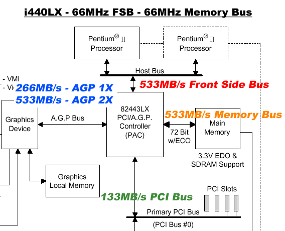
Here we have an old 440LX setup with a 66MHz FSB and a 66MHz memory bus which are the official operating conditions for the Celeron. Because both the FSB and the memory bus are 64-bits wide and run at 66MHz, they both provide 533MB/s of bandwidth to/from the North Bridge. Now if your CPU just communicated to your memory all the time and didn't have to compete with any other devices in the system for that 533MB/s of bandwidth all would be good.
Unfortunately, once you factor in the 533MB/s of bandwidth an AGP 2X graphics card is capable of sustaining and the 133MB/s of the PCI bus, all of the sudden that 533MB/s throughput to the memory doesn't seem to be all that much. But as long as the graphics subsystem and the PCI bus aren't taking up too much memory bandwidth, you should be fine.
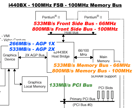
The 440BX platform helped to avoid any possible bottlenecks by increasing the FSB/memory bus frequencies from 66MHz to 100MHz this effectively increased the available memory bandwidth by 50% to 800MB/s.
At the time when the 440LX - 440BX transition was being made, the benchmarks available as well as the games being played did not illustrate a need for something faster than a 66MHz FSB/memory bus. The reason behind this was that they simply weren't stressing all of the memory masters and thus weren't saturating the 800MB/s of memory bandwidth allowed by the 100MHz FSB/memory bus which made it seem as if there was no tangible performance difference between the 66MHz LX platform and the 100MHz BX platform.
Memory Bus - 66MHz vs 100MHz
In order to illustrate the real world performance improvement achieved by using a 100MHz memory bus vs a 66MHz memory bus we used our VIA Apollo Pro 133A test platform which allows us to set the memory bus to 100MHz even if the FSB frequency is set to 66MHz.
In the following tests the CPU used is an Intel Celeron 600 running at 66MHz x 9.0, for the 100MHz memory bus tests the memory bus ran at 100MHz and for the 66MHz memory bus tests the memory bus obviously ran at 66MHz.
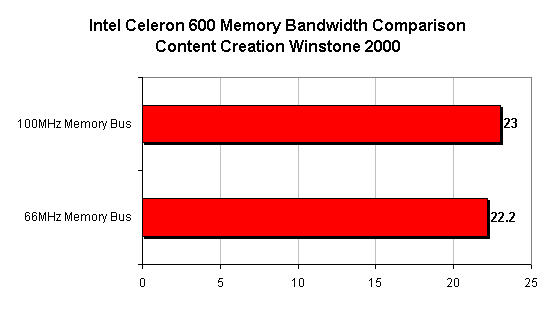
In spite of the multitasking nature of the Content Creation Winstone 2000 benchmark, the performance difference between the 100MHz memory bus and 66MHz memory bus is only about 4%. This illustrates the point that for most home office/business tasks, a 66MHz memory bus is still enough to perform at a reasonable level.
Considering the market Intel is targeting with the Celeron, this makes sense since most of the users in the Basic PC market aren't going to be running heavy 3D applications, etc...
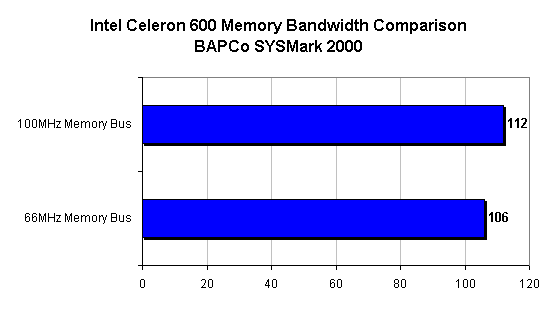
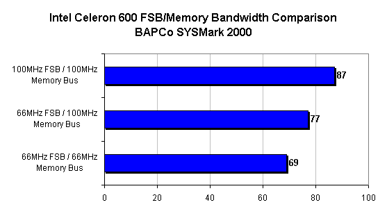
Moving to the 100MHz memory bus results in a 6% improvement here which still isn't phenomenal but it's definitely more than we observed in the CC Winstone 2000 benchmark.
The reason behind the somewhat larger performance difference here is because SYSMark 2000 runs a variety of applications including SOHO applications but also 3D rendering, voice recognition and other such applications that are much more memory bandwidth intensive which is why the performance difference is larger here while at the same time not incredible.
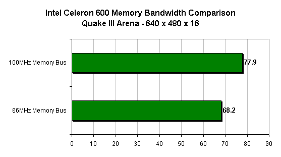
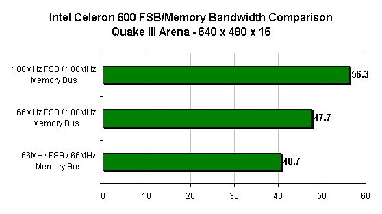
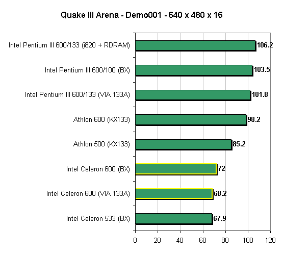
Here is when we begin to see some of the real performance difference. Simply moving to the 100MHz memory bus in Quake III provides for a 14% performance improvement.
The reason the improvement is so noticeable here is because Quake III, unlike SYSMark 2000, is a very specific benchmark in that we aren't averaging in the performance of the setup under business applications with the performance of the setup under Quake III. Combine that with the fact that Quake III is very memory/graphics intensive (it is a game after all) and you get a pretty big difference simply by using a 100MHz memory bus.

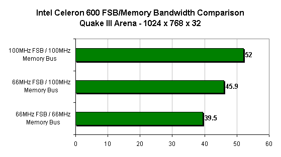
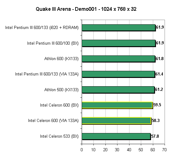
At 1024 x 768 x 32 the GeForce in our test bed is acting as a limiting factor in the benchmark but even in spite of the fill rate limitation here we still see a 6% improvement in performance caused by the 100MHz memory bus. At such a high resolution there is definitely more AGP texturing going on which could be contributing to the still measurable performance difference between 66MHz vs 100MHz.
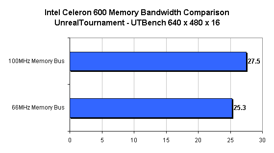
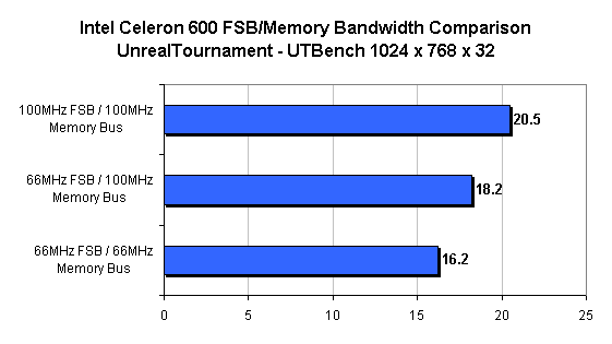
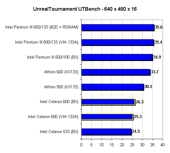
UnrealTournament is much like Quake III although limitations in the Unreal Engine cause the performance difference here to be around 9%.
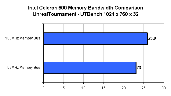
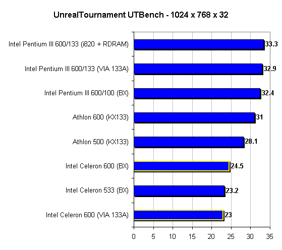
The performance difference at the higher resolution is slightly higher than at 640 x 480 x 16 most likely because of limitations of the Unreal Engine but needless to say, a 13% performance improvement over the 66MHz memory bus is definitely noticeable.
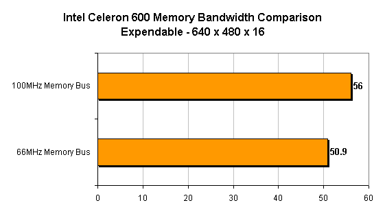
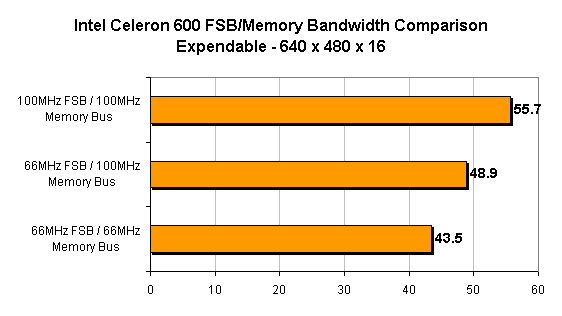
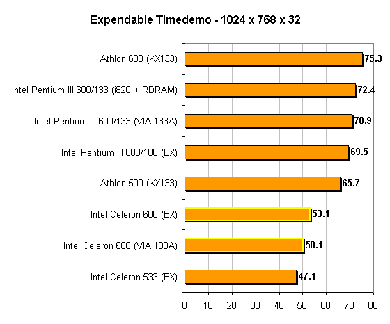
Under Expendable we get a 10% improvement in performance which is in-line with what we have been expecting courtesy of the initial Quake III scores.
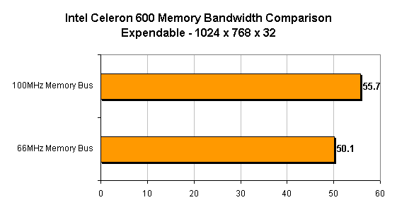
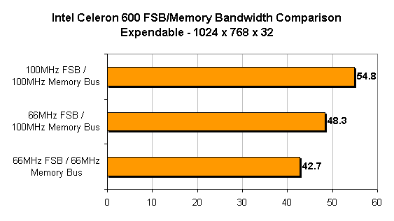
The situation is virtually identical at 1024 x 768 x 32
FSB - 66MHz vs 100MHz
Since all Celerons have locked clock multipliers, it is impossible to run a Celeron 600 at 66MHz x 9.0 and 100MHz x 6.0 to test the effects of the 100MHz FSB in addition to the 100MHz memory bus on performance.
Luckily, since the new Celeron only differs from the Pentium III in that it features 128KB of L2 cache instead of the 256KB on Pentium III, by disabling the L2 cache on the Celeron and on the Pentium III we can put together a pretty nice match-up to compare the effects of the 100MHz FSB on the Celeron in order to find out if this is a limitation of the design.
We used the same VIA 133A platform from before so that we could adjust the memory bus frequency in addition to the FSB frequency and the L2 cache was left disabled in order to level the playing field. Disabling the L2 cache also makes the system more memory dependent because the CPU has no level 2 cache to go to for data and thus must go directly to system memory. While this does somewhat exaggerate the effects of the memory bus on performance it is necessary in order to illustrate the point.
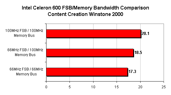
We already found out that going to a 100MHz memory bus would give us a small performance improvement under CC Winstone 2000 from the earlier tests but by increasing the FSB to 100MHz as well the performance improvement more than doubles offering a 16% improvement over the 600/66MHz clock of the Celeron 600.
Although the Pentium III 600E has a 128KB L2 cache advantage over the Celeron 600 most of its performance improvement should come from the 100MHz FSB and 100MHz memory bus rather than the larger L2 cache.
Under SYSMark 2000 approximately 11% of the 26% improvement in performance is due to the 100MHz memory bus, the remaining 15% is due to the increased FSB frequency.
Going from a 66MHz FSB and 66MHz memory bus up to 100/100MHz results in a 38% improvement in performance under Quake III with 17% of that due to the increase in the memory bus and the remaining 21% due to the increase in FSB frequency.
While the performance difference isn't as dramatic at the higher resolution it is still fairly noticeable at 31%. With just about half of that increase being due to the increase in memory bus frequency, the other half being attributed to the increased FSB frequency.

We get a similar situation under Unreal Tournament, the percentages are a little different but overall the trend continues. The 100/100MHz setup provides for a 28% improvement over the 66/66MHz setup.
Nothing new here, just about half of the performance increase comes from the increase in memory bus frequency and the other half comes from the increase in FSB frequency.
The Test
|
Windows 98 SE Test System |
|||||
|
Hardware |
|||||
|
CPU(s) |
Intel
Celeron 600 |
Intel Pentium III 600EB
|
AMD Athlon 600
AMD Athlon 500 |
||
| Motherboard(s) | ABIT BE6 | AOpen AX6C | ASUS P3V4X | ASUS K7V-RM | |
| Memory |
128MB PC133 Corsair SDRAM |
128MB
PC800 Samsung RDRAM
|
128MB
PC133 Corsair SDRAM
|
128MB
PC133 Corsair SDRAM
|
|
| Hard Drive |
IBM Deskstar DPTA-372050 20.5GB 7200 RPM Ultra ATA 66 |
||||
| CDROM |
Phillips 48X |
||||
| Video Card(s) |
NVIDIA GeForce 256 32MB DDR (default clock - 120/150 DDR) |
||||
| Ethernet |
Linksys LNE100TX 100Mbit PCI Ethernet Adapter |
||||
|
Software |
|||||
|
Operating System |
Windows 98 SE |
||||
| Video Drivers |
|
||||
|
Benchmarking Applications |
|||||
| Gaming |
GT
Interactive Unreal Tournament 4.04 UTbench.dem |
||||
| Productivity |
BAPCo SYSMark 2000
Ziff Davis Content Creation Winstone 2000 |
||||
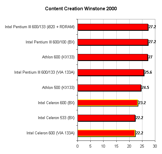
After explaining what the bottlenecks the Celeron will face actually are it is time to see how it stacks up to the competition. As you can see, the limitations are definitely evident as the Pentium III 600E manages to come out on top of the Celeron 600 by about 17%. But as we already explained, this 17% differential is because of the memory/FSB frequencies and not the L2 cache size advantage of the Pentium III.
For comparison's sake, a regular Pentium III 550 (Katmai core) with 512KB L2 cache running at 1/2 clock speed on our 133A test bed pulls in with a score of 22.8 which is higher than the new Celeron at 600MHz on the same test bed. So even with a slower L2 cache, the older Pentium III can outpace the newer Celeron because of the limitations of the Celeron's 66MHz bus.
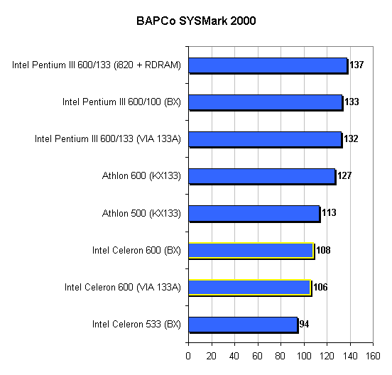
There is a similar situation under SYSMark 2000, with the 600E coming out on top of the Celeron 600 by about 23% which is, once again, due to the 100MHz bus speed advantage.
In this particular test, an older Pentium III 550 on our VIA 133A platform came out with a score of 112, faster than even the Celeron 600 on a BX setup. If you happen to own an older Pentium III and are looking for an upgrade, the Celeron isn't the way to go.
As we predicted in our 66MHz vs 100MHz sections earlier in the review, the gaming performance of the Celeron pales in comparison to its 100MHz FSB counterparts. An older Pentium III would still be faster as our old 550 was able to hit around 80 fps in this test on our 133A test bed.
We get a similar situation under UnrealTournament which, as a game, is fairly dependent on a fast memory/system bus.

Conclusion
The new Celeron is definitely not the most impressive processor out there but then again it wasn't meant to be. The Celeron is and has always been aimed at the "Basic PC" market segment not at the performance market segment and especially not at the high-end market segment.
Considering the fact that the Celeron, as a 66MHz FSB part could still be used in an older LX motherboard provided that the manufacturer provided BIOS support for the chip, the CPU does an excellent job at offering good entry level performance at a not so high cost.
For those of you that are looking to pick up one of these new Celerons because of their sub-$200 price tag but are disappointed by the performance, your best bet is to pair up the new Celeron with a 133A motherboard and bump memory bus frequency up a notch to at least 100MHz.
If you happen to be a first generation Pentium III owner looking for an upgrade to a processor with a bit more kick, the Celeron is definitely not the way to go. Your 'old' Pentium III is a faster solution because of its 100MHz FSB frequency and thus you should only look towards the new Coppermine Pentium IIIs as a potential upgrade path or AMD's Athlon if you don't mind replacing your motherboard.
While we had expected the new Celeron to be an overclocking madman, it will take just a little bit longer for that dream to come true. We were only able to get our hands on a 600MHz sample which, because of its 9.0x clock multiplier would only be able to hit 900MHz when used with a 100MHz FSB setting. Although an overclock like this may be possible as yields improve, our sample wasn't able to do it. A Celeron at 900/100MHz would be just about as fast as a Pentium III at 900MHz in most situations, in spite of the smaller L2 cache. We will be publishing an Overclocking the Celeron guide shortly to describe the performance benefits associated with overclocking these new Celerons.
With AMD's Spitfire due out shortly the "Basic PC" market segment is about to get interesting, with the new Celerons being crippled by the 66MHz FSB/memory bus to the point where the older Pentium IIIs are faster than them, an AMD Spitfire with 128KB of L2 cache could easily take the performance crown from Intel in the low-end market. At the same time, there is nothing to say that the Spitfire isn't crippled in another way as well...
How it Rates
|
AnandTech CPU Rating |
|
|
Rating
(x/10)
|
|
|
Performance
|
5.0
|
|
Features
|
7.0
|
|
Price
|
8.5
|
|
Availability
|
7.5
|
| Overall Rating - Not an Average - Click here to find out why |
7.0
|


