Original Link: https://www.anandtech.com/show/1
FIC PA-2013 2MB Cache Version
by Anand Lal Shimpi on December 16, 1998 1:10 PM EST- Posted in
- Motherboards
No one could've predicted how well the Super7 market would do back in 1997. There was no certainty that AMD would be able to follow up their claims of a true upgrade path for all Super7 users, and no one had seen evidence of a working "K6-3D," so why would a manufacturer spend their time and money on a risky market they were unsure of?
In 1998 however, things changed incredibly, the Super7 market proved to be a profitable one, and manufacturers either kicked themselves for not jumping on the bandwagon at the start (cough-ABIT-cough) or smiled knowingly as their Super7 products took off in sales.
As with the release of BX motherboards, Super7 motherboards came in generation waves, with each following generation bringing a new feature or two to the table, and in the tradition of evolution, FIC brought their next generation Super7 motherboard to the eyes of the eagerly awaiting market, it's about time that you all met the Super7 with K6-3 written all over it. What does that mean? Well, the K6-3 will come with its own integrated 256KB of L2 cache, and will cause the motherboard's on-board cache to be bumped down to a Level 3 cache...so picture this for a moment: a K6-3 running at 450MHz, 64KB of L1 cache, 256KB of L2 cache, and 2MB of L3 cache courtesy of the new FIC PA-2013. Not a bad dream, but how much of a performance increase will that 2MB L3 cache provide you with, and what happens between the time between now and when the K6-3 is released? Will you enjoy the board or will it be a pain to deal with? Let's find out as AnandTech gives you an exclusive look at the new FIC PA-2013 VIA MVP3 Super7 motherboard with 2MB of cache. It's finally here...
New Anand Tech Report Card Rating
78/C
Do not compare newer ratings to older ones, the newer ratings are much more aggressive
| CPU Interface | Super Socket-7 |
| Chipset | VIA MVP3 |
| L2 Cache | 2048KB |
| Form Factor | ATX |
| Bus Speeds | 60 / 66 /
68 / 75 / 83 / 95 100 / 112 / 124 |
| Clock Multipliers | 1.5x - 5.5x |
| Voltages Supported | 1.8v - 3.5v (0.1v increments) |
| Memory Slots | 3 168pin DIMM Slots (EDO/SDRAM) |
| Expansion Slots | 1 AGP
Slot 4 PCI Slots (4 Full Length) 2 ISA Slots (1 Shared / 2 Full Length) |
| BIOS | Award BIOS |
The Good
| Like the 512KB/1MB versions of the PA-2013, the 2MB board comes outfitted with a 4/2/1 expansion slot configuration (PCI/ISA/AGP) and 3 DIMM slots. The peripheral and memory expansion slots are laid out on an ATX PCB (Printed Circuit Board) approximately the size of most Pentium II BX boards like the ASUS P2B and the Epox P2-112A. The 4 - 512KB L2 cache chips take the place of the four chips present on the 1MB board and run adjacent to the Socket-7 IC in the form of an L-shape. The 2MB of L2 cache starts off by enabling the VIA MVP3 chipset's 508MB cacheable memory area, up from the 254MB of the 1MB version and the 127MB of the 512KB version. | 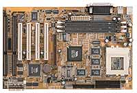 |
The layout of the board hasn't changed at all since the original introduction, the ATX power connector is found at the top of the board placed almost flush against the first DIMM slot, and wedged next to the I/O ports. Surrounding the Socket-7 IC and around the memory slots are a few small to mid-sized capacitors, with a great number of them populating the area around the switching voltage regulators.
| Like all newer MVP3 based motherboards, the PA-2013 ships from the factory with revision 'CE' of the chipset which eliminates the problems the chipset had with i740 based graphics accelerators. The CE North Bridge is what drives the AGP 2X compliant port which is located just left of the chip itself. A little peek into the future is possible with the PA-2013, looking to the area just below and to the left of the AGP slot AnandTech noticed a little label for a Front-USB port 'F-USB' with a connector next to the text, unfortunately the connector was hammered in, but it does look like we can expect to see some Front USB ports on more motherboards in the future. Wonder how long it would take to get those USB ports off of the ATX Back Panel and create a new opening on the front of most cases... | 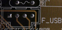 |
FIC is up to their usual standards with the motherboard manual bundled with the PA-2013. The written documentation includes the settings for all officially supported bus speeds as well as the overclocked 75/83/112/124MHz settings for pushing your luck. Clock multipliers ranging from 1.5x to 5.5x are also documented, not to mention the excellent support for core voltage settings ranging from 1.8v to 3.5v in 0.1v increments. FIC also includes a fairly complete table of CPU settings for the most popular chips in the manual which is a handy tool for first time builders, or even those who are just looking to get a kick out of reading up on older CPU settings ;)
The PA-2013's stability was not sacrificed under normal operation as a result of the 2MB of L2 cache, as the AnandTech tests proved, the system crashed a total of 4 times over a 24 hour testing period while running a variety of business and 3D gaming applications. Like the original PA-2013, the 2MB version does come with Trend's ChipAway BIOS Virus Protection program that prevents boot sector viruses from loading even before your system starts up your operating system, just an added safety feature which may come in handy in this download-driven Internet world.
| The PA-2013's performance rose an average of 3% in business applications, with performance increases peaking at the 5 - 7% level, placing it at the top of the Super7 motherboard performance charts. As you might be able to guess, the improvements in 3D games is virtually un-noticeable, so if you have a PA-2013 or another Super7 board right now that you're happy with, there is no point to upgrading to this 2MB version simply because of the performance increases. Even L2 cache dependent games such as Unreal didn't receive any improvement in performance as a result of the larger cache, in this case, their performance was being limited by the actual speed of the cache, not the size. | 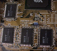 |
The Bad
As with the older PA-2013's, five PCI slots would've made this board the dream of many users, unfortunately, in order to conserve space, the PA-2013 was only outfitted with 4. The positioning of the Socket-7 CPU interface isn't ideal for cooling as the path of airflow from your ATX power supply will pass directly over your memory banks, leaving your CPU fan to take care of all of the cooling duties for your CPU. The positioning of the ATX power connector is also a bit of a pain to deal with, especially if you have all three SDRAM banks occupied.
Now here's the real problem with that 2MB L2 cache, the board wasn't reliable enough at any overclocked FSB speeds (112MHz or 124MHz) most likely as a result of the quality of the L2 cache chips. Where the older PA-2013's outfitted with 512KB or 1MB of L2 cache could perform quite reliably at 112MHz, the 2MB version AnandTech tested couldn't. In the future this problem may be addressed and corrected with higher quality L2 cache, however that won't come without an added cost to the end user, making overclocking on this board, other than with the 100MHz FSB, undesirable.
USB Compatibility
Number of Universal Serial Bus Root Ports: 2
USB IRQ Enable/Disable in BIOS: Yes
USB Keyboard Support in BIOS: Yes
BIOS Settings
FIC PA-2013 Chipset Features Setup |
||||
| Item | Settings | |||
| FPM | EDO/SDRAM 60/66MHz Bus | EDO/SDRAM 75/83/100/112MHz Bus | Safe | |
| Video BIOS Cacheable: | Enabled | Enabled | Enabled | Disabled |
| System BIOS Cacheable: | Enabled | Enabled | Enabled | Disabled |
| Memory Hole At 15Mb Addr.: | Disabled | Disabled | Disabled | Disabled |
| DRAM Page-Mode: | Enabled | Enabled | Enabled | Disabled |
| Sustained 3T Write: | Enabled | Enabled | Enabled | Disabled |
| Cache Pipeline: | Enabled | Enabled | Enabled | Enabled |
| DRAM Read Pipeline: | Enabled | Enabled | Enabled | Disabled |
| Read Around Write: | Enabled | Enabled | Enabled | Disabled |
| Memory ECC Check: | Disabled | Disabled | Disabled | Disabled |
| Bank 0/1 DRAM Timing: | 60 ns | Turbo | Turbo | Normal |
| Bank 2/3 DRAM Timing: | 60 ns | Turbo | Turbo | Normal |
| Bank 4/5 DRAM Timing: | 60 ns | Turbo | Turbo | Normal |
| SDRAM Cycle Length: | 3 | 2 | 2 | 3 |
| SDRAM Bank Interleave: | Disabled | 4 Bank | 4 Bank | Disabled |
| SDRAM MD-to-HD Pop + 1T: | Enabled | Disabled | Enabled | Disabled |
| Aperture Size: | 64M | 64M | 64M | 8M |
| AGP-2X Mode: | Enable | Enable | Enable | Disable |
| Spread Spectrum: | Enabled | Enabled | Enabled | Disabled |
Recommended SDRAM
Recommended SDRAM: Mushkin SEC -GH PC100
SDRAM; Memory Man SEC -GH PC100 SDRAM
SDRAM Tested: 1 x 64MB Mushkin PC100 SDRAM; 1 x 64MB Memory-Man PC100 SDRAM
Manufacturer: The Memory Man
Purchase Web-Site: http://www.memory-man.com
Manufacturer: Mushkin
Purchase Web-Site: http://www.mushkin.com
The Test
In recent times, choosing a motherboard cannot be completely determined by a Winstone score. Now, many boards come within one Winstone point of each other and therefore the need to benchmark boards against each other falls. Therefore you shouldn't base your decision entirely on the benchmarks you see here, but also on the technical features and advantages of this particular board, seeing as that will probably make the greatest difference in your overall experience.
How I Tested
Each benchmark was run a minimum of 2 times and a maximum of 5 times, if the motherboard failed to complete a single test within the 5 allocated test runs the OS/Software was re-installed on a freshly formatted Hard Drive and the BIOS settings were adjusted to prevent the test from failing again. All such encounters were noted at the exact time of their occurrence.
Business Winstone 98 & 3D Winbench 98 was run at each individually tested clock speed, if reliable scores were achieved with the first two test runs of the suite an average of the two was taken and recorded as the final score at that clock speed. If the test system displayed erratic behavior while the tests were running or the results were incredibly low/high the tests were re-run up to 5 times and an average of all the test runs was taken and recorded at the final score at that clock speed
All video tests were conducted using an AGP video accelerator
No foreign drivers were present in the test system other than those required for the system to function to the best of its ability
All foreign installation files were moved to a separate partition during the test as to prevent them from effecting the test results
All tests were conducted at 1024 x 768 x 16-bit color
3D Winbench 98 tests were double buffered and conducted at 800 x 600 x 16-bit color
Test Configuration |
|
| Processor(s): | AMD K6-2 350 AFR Intel Pentium MMX 233 Cyrix M-II 300 |
| RAM: | 1 - 64MB Memory Man PC100 SDRAM DIMM |
| Hard Drive(s): | Western Digital Caviar AC35100 - UltraATA |
| Video Card(s): | Matrox Millennium G200 (8MB SGRAM - AGP) |
| Bus Master Drivers: | Microsoft Win98 DMA Drivers |
| Video Drivers: | MGA Millennium G200 Release 1677-411 |
| Operation System(s): | Windows 98 |
| Motherboard Revision: | FIC PA-2013 Revision 2.0 (2MB) |
Ziff Davis Winstone 98 - Windows 95 Performance |
|
| Business | |
| AMD K6-2 350 - 100MHz x 3.5 | 25.4 |
| AMD K6-2 300 - 100MHz x 3.0 | 24.2 |
| AMD K6-2 300 - 66MHz x 4.5 | 22.0 |
| Intel Pentium MMX 200 - 100MHz x 2.0 | 18.7 |
| Intel Pentium MMX 233 - 66MHz x 3.5 | 18.1 |
| Cyrix M-II 300 66MHz x 3.5 | 22.7 |
According to AMD, and with the BIOS that shipped with AnandTech's PA-2013, the K6-3 should work perfectly fine on the newly revised PA-2013 as well as all of the older revisions of the board. If you couple that with the 2MB of cache this board brings with it, and the 3% performance increase that it allows, the PA-2013 still retains its original value. However be weary of two things, the number of PCI slots on the board will quickly fill up, and you may be cheating yourself out of the 112MHz FSB setting with this board unless the quality of the on-board cache can be improved...then again, with the integrated L2 cache of the K6-3, the speed of your L3 cache won't really matter all that much. An pretty good job as a board to stick a K6-3 on, but as for a K6-2 owner's overclocking wonder, the 2MB PA-2013 may end up being more of a disappointment.
AnandTech Motherboard Rating |
|
| Business | |
| Performance | 85% |
| Price | 85% |
| Ease of Use | 75% |
| Overclocked Stability | 65% |
| General Stability | 75% |
| Quality | 75% |
| Documentation | 85% |
| Reliability | 82% |
| Overall Rating | 78% |
The
New Rating System
Each motherboard is rated in 8 areas, Performance, Price, Ease of Use, Overclocked
Stability, Stability, Quality, Documentation, and Reliability.
Do not compare newer scores to older ones, the newer scores are much more aggressive
Performance - How well the motherboard compares to others in its class
Price - How competitive the price of the motherboard is when compared to others in its class
Ease of Use - How easy it is to setup the motherboard, jumper settings, jumperless configuration etc...
Overclocked Stability - How stable the motherboard is at overclocked CPU/Bus speeds
Stability - How stable the motherboard is at normal CPU/Bus speeds
Quality - How much effort went into producing the motherboard
Documentation - How helpful is the manual and bundled support manuals
Reliability - How long will this motherboard last, will it fail? Deals with quantity/size of capacitors, known bugs, etc...
Overall Rating - an average of the eight above areas


